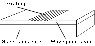
The basic principle of the OWLS technology is that linearly polarized light (He-Ne laser) is coupled by a diffraction grating into the waveguide layer, provided that the incoupling condition is fulfilled.
The incoupling is a resonance phenomenon, that occurs at a precise angle of incidence which depends on the refractive index of the medium covering the surface of the waveguide. In the waveguide layer the light is guided by total internal reflection to the ends where it is detected by photodiodes. By varying the angle of incidence of the light the mode spectrum can be obtained from which the effective refractive indices are calculated for both the electric and magnetic modes. OWLS is a label-free, real-time technology for investigating adsorption, binding and adhesion processes.
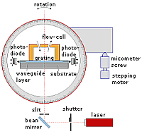
Schematic drawing of the system
Learn more about the OWLS system
Measured spectra
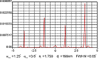 The graph shows a typical light mode spectra of an OW 2400 sensor
The light intensity is measured with the photo detectors as the angle of incidence of the laser light is varied from -6o to +6o.
From the measured mode spectra, the BioSense application calculates the waveguide layer’s or the covering medium’s physical parameters such as thickness, optical refractive index, density and more.
Theory and Models
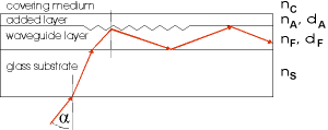
Ray-optic representation of a coupled and guided wave
Electromagnetic field distribution for a zeroth mode
See the demonstration video on how the laser light is incoupled into the planar waveguide when the optical grating is illuminated at a certain, resonance angle of incident.
Calculation:
- The incoupling angles a(TE), a(TM) for electric and magnetic modes are evaluated from the measured spectra
- The effective refractive indices N(TE), N(TM) of the waveguide structure are calculated on the basis of incoupling condition.
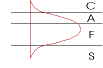
- Supposing that N(TE), N(TM) has been calculated and the optical parameters of the waveguide layer (nF,dF), of the substrate (nS), of the covering medium (nC) are known, the refractive index (nA) and the thickness (dA) of the added layer can be calculated.
- Using the model that the refractive index in the adsorbed layer linearly depends on the concentration of the adsorbed material, the mass per area of the adsorbed material can be calculated.
Sensor chips
The optical waveguide sensor chips are made of SOL-GEL technology and are produced by us.
Technical specification of the OW sensor chips
Sensing principles
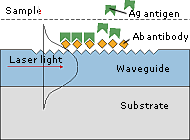
Immunosensor
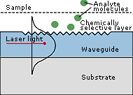
Monomolecular chemoresponsive coating, which consists of immobilized antibody (Ab) molecules, that bind the corresponding antigen (Ag) molecules.
Chemosensor
With a typically 0,1-1 mm thick chemoresponsive layer whose refractive index is changed by binding the analyte molecules.